Datasheet4U Logo Datasheet4U.com

ADP1196 Datasheet High-Side or Low-Side Load Switch

Manufacturer: Analog Devices

General Description

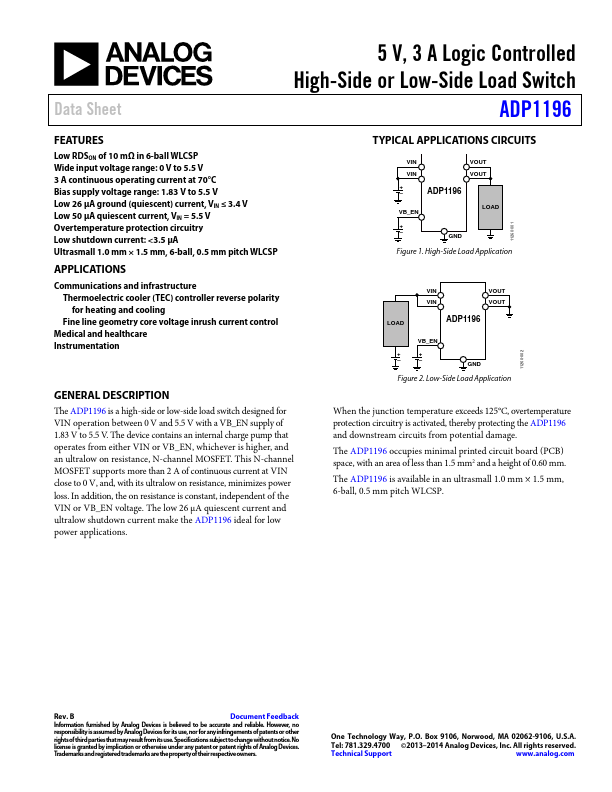
The ADP1196 is a high-side or low-side load switch designed for VIN operation between 0 V and 5.5 V with a VB_EN supply of 1.83 V to 5.5 V.

The device contains an internal charge pump that operates from either VIN or VB_EN, whichever is higher, and an ultralow on resistance, N-channel MOSFET.

This N-channel MOSFET supports more than 2 A of continuous current at VIN close to 0 V, and, with its ultralow on resistance, minimizes power loss.

Overview

Data Sheet 5 V, 3 A Logic Controlled High-Side or Low-Side Load.

Key Features

  • Low RDSON of 10 mΩ in 6-ball WLCSP Wide input voltage range: 0 V to 5.5 V 3 A continuous operating current at 70°C Bias supply voltage range: 1.83 V to 5.5 V Low 26 µA ground (quiescent) current, VIN ≤ 3.4 V Low 50 µA quiescent current, VIN = 5.5 V Overtemperature protection circuitry Low shutdown current:.